English Japanese
I made TLS speaker system just one years before, the sound is very good, but I am not pleased with its low efficiency, so I decide to make a high power amplifier.
Basically, it becomes difficult to make an amplifier if its power is larger. This is truth, but recently a hundred watts is not so difficult for the solid state amplifier, althogh in old days 100W had been difficult because of the lower semiconductor's maximum ratings.
However, for the tube amplifier it is still difficult to achieve 100W.
There are many kinds of power tubes for the high power amp. For example, EL34, 6550/KT88, maybe EL156 is enthusiastic choice, 8417 will be maniac, or I have four PL519 stock.
··· Suddenly, I have found the important point.
The voltages should be too high for ordinary parts.
The electric capacitors over 500V ratings are not easy to buy, and it is very expensive even if we can get.
The output transformer is also the problem, because the high +B voltage means high swing voltage of the transformer with high impedance. That means very high inductance is required and also many turns should be wounded. By this method, the higher response tends to be worse, so the special winding method is sometimes used, so the cost of iron is higher.
Power transformer is also the problem. In japan, I cannot find the suitable one, so probably the custom made iron will be required.
On the other hand, if the voltage is low, in other words if low impedance and high current, there is no problem. The transformer turns can be also reduced (I mentioned this point later).
So, I decide to make parallel PP with EL34.
I can use the cheap power transformer, which is on sale at Noguchi trans, and it has a pretty good performance.
Although, I had to pay the additional cost in order to buy a carry cart, as it is too heavy to bring it from Akihabara ;)
I had made STC-VX, but it did not work well, so I remake with different circuit topology.
At first, I made with this topology.
The basic idea was born from Kamijo-san, and I modified it.
Simply speaking, the local feed back loop with STC-VX method by the divided resistors, and additional stage differential amp.
STC-VX method may not be easy to understand. Please find here its equivalent circuit analysis of STC-VX method.
Unfortunately, it did not work stable enough how I adjust the constants.
If decreasing the gain by inserting the resistor to the cathode, it could be stable, but it is stupid idea because there is no advantage of this circuit.
When I connected the both cathodes of second stage to the ground with capacitor, parasitic oscillation had been found without any feed back, because such a circuit has a common mode gain for high frequency.
In real, the differential amplifier can suppress this error because it has high common mode rejection ratio. The differential amp gain is decreased, but many advantages.
But, this stage should be AC differential amp or the deep current feed-back (decreasing the gain) is required for the DC balance.
Maybe, there is no need to say, the simple conventional differential amplifier cannot use for this stage, as the first stage DC offset and drift should be smaller than 0.01V because of the second stage DC gain.
The input resistor of the first stage is also employed for stopping the parasitic oscillation.
Input line is shiled cable, as it oscillated with normal wire. And centre pin should be grounded, for using high gm tube.
If decreasing the current of the first stage, parasitic oscillation may be rejected, but second stage anode swing voltage is very high because of STC-VX feed-back, so the Miller effect can be found strongly.
The series grid resistors of EL34 final stage are also used to suppress the parasitic oscillation.
I had found the oscillation of the regulated power supply, so whilst one month, I had fought with oscillation of this circuit :-(
However, I cannot make stable amp with good quality, so I gave up and making with new circuit design.
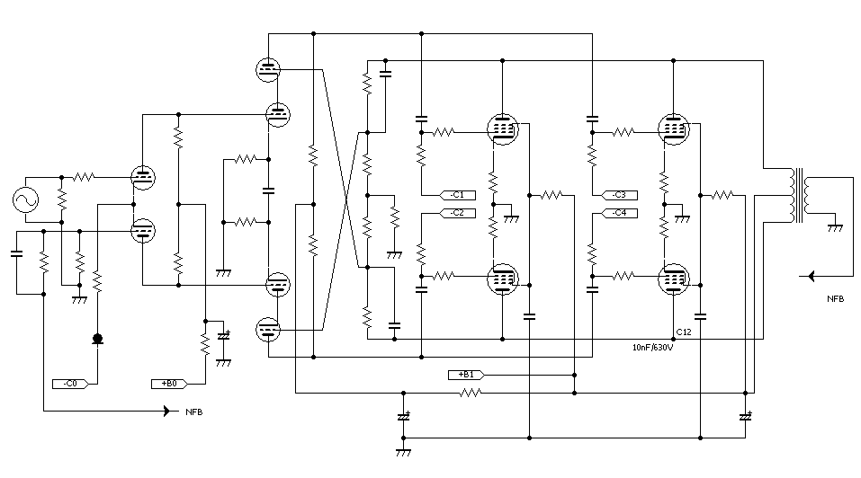
I changed the circuit completely, and you can find it below.
The circuit has a local feed back loop with using double balanced differential amplifier.
The double balanced differential amp is sometimes used for radio wave circuit, but in my design balanced feed back is performed to the similar circuit as an fT doubler with Gilbert cell.
The schematics shows its principle but not real one, so it should be AC coupling for the second stage local feed back because of the DC balance.
I think the circuit itself is easy to understand, so there is no need to write down the equivalent circuit for calculation, but please be care that the both of 1st stage and 2nd stage are feed backed, so the input of differentials are the common mode.
In other words, open loop gain becomes half, and the swing voltage of the 2nd stage becomes quite large.
This is the reason why the constant current is used for the common cathode of second stage, even though the VX amp does not need it.
Clearly, the open gain of this circuit will be lower than STC-VX.
However, as I already mentioned, STC-VX does not work in stable without current feed-back, so substantially this feed-back gain is larger than previous one.
The biggest reason that this circuit is more stable than previous one, is the output resistance of the 2nd stage is far lower.
Of cause I had simulated before making previous circuit, but sometimes we cannot find everything from the computer simulation.
The employed tube number is the same as above VX, and the number of tubes are also same as Wiliamson amp, that the late Mr. Isamu Asano (he had been Chief director of Japan Audio Society) loved.
In short, deep feed-back requires many tubes, but the amp stages are less than Wiliamson's, because of differential amps.
Total feed-back gain is larger than Wiliamson's, but my amp has local feed-back, so the feed-back gain of whole loop is less.
It will be possible to realise the circuit similar to the "STC-MX" with same number of tubes, but the new amp circuit has two advantages.
One is less number of stages, so that we can make stable feed-back, and the other one is, the schematics looked nice, isn't it? ;)
Bob Widlar's design is the the standard operational amplifier style, and it has a very low frequency dominant pole and quite high DC gain for the feed-back. By this method, the amplifier allows stable feed-back, due to always 90 degree phase margin, in ideal.
He designed very old IC OP amp 702, 709 and so on, but his superior architecture has been incessantly succeeded still now.
R. J. Widlar, "Design techniques for monolithic operational amplifiers,"
IEEE Journal of Solid State Circuits, vol. SC-4, pp. 184-191, 1969.
I adopted this idea for my new amplifier. However, of cause it is difficult to get 100dB feed-back gain with tube amp, but I adopted his underlying concept, very stable feed-back by the phase of asymptotic 90 degree.
(Although the traditional tube amp feed-back method might be OK, since the major loop feed-back gain of my amp is not so large.)
My amp has local freed-back, and I added the time constant to this local feed-back circuit, which makes stable dominant pole, like as Widlar design.
The biggest reason that the Widlar style is not so popular for the tube amp is the output transformer. The output transformer has a pole at 100 to 200kHz with second order complex pole.
Therefore, the iron's phase rotates more than 90 degree, and it close to 180 degree.I employed lag-lead compensator to reject this issue.
The Wiliamson's amp also used lag-lead compensator, as it is the easiest method for deep feed-back with including iron. (if limiting classical control technology theory;)
I do not designed this method in real, but I would like to explain the design of lag-lead compensator with classical control technology using the Bode chart.
In real, the output transformer has the 2nd order complex pole. On the other hand the Bode chart design is normally used for the poles on the real axis, but please find the underlying principle for this design.
I employed the iron which characteristic is like as below figure 1.
![]() Fig. 1
Fig. 1
The real high frequency response will be changed by the drive impedance, but I explain those characteristics later.
General non-inverting feed-back amplifier with parallel capacitor, like as below figure 2;
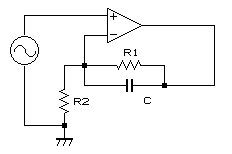 Fig. 2
This can be lag-lead compensator. It can be analyzed easily
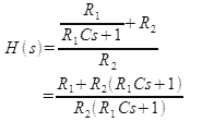 · · · eq.1
The gain of this circuit is close to the 1 at high frequency in theory, but normally high gain becomes lower because of another pole.
Therefore the lowest gain (the flat position in figure 3) should be 0dB (gain=1), but we can change it with adding the series resitor R3 to the capacitor C, like as below equation 2.
![]() · · · eq.2
· · · eq.2
By this method, we can get the gain higher than 1.
Please find below figure 3, the zero point of this circuit should be the cut off frequency of the transformer, and from the gain of the amplifier, we can get the pole of the amplifier by the 6dB/oct line from above zero point.
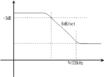 Fig.3
Fig.3
Then, we can get the function which is similar to the 1st order, that is Fig 4 which synthesized from Fig 1 and Fig 3.
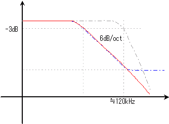 Fig.4
Fig.4
From above figure 2 and 3, it is easy to understand that the dominant pole should be defined from the feed-back gain .
In real, of cause the transformer has complex poles and there is another pole for the amplifier, so the transfer function is not so simple like as these figures. I simulated 7 poles, but real poles may be more.
By this circuit, I found slightly unstable indication from response, so I added the another lag-lead compensator to the major feed-back loop.
I calculated with mathematical CAD.
Real transformer characteristic at high frequency will be changed by the drive impedance value, but Mr. van der Veen, who designed this transformer, wrote a paper which is written in the details of transfer function and its parameters, so I used his method for my calculation.
ir. Menno van der Veen; "Theory and Practise of Wide Bandwidth Toroidal Output Transformers";
preprint 3887, 97th AES Convention San Francisco
The final simulation Bode chart can be shown below figure.
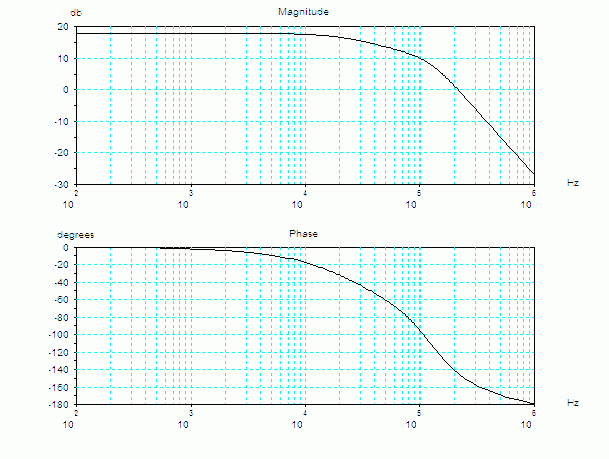
The phase margin seems to be enough, but real circuit may be different from this simulation ;)
The maximum swing voltages of each stage could be different by the frequency because of the local feed-back loop.
The gain of 2nd stage and final stage is defined by the local feed-back, which is almost twenty times, but the high frequency gain is decreased by the lag-lead compensator.
Therefore, the high frequency swing voltage of the 1st stage becomes larger than lower frequency. Similar phenomenon is always found if another phase compensation, the swing current may be larger instead of the voltage.
However the biggest difference to the another phase compensator like as famous Williamson amp is my method increases local feedback gain at high frequency.
The local feed back closed loop gain (the 2nd and final stage) is 20 times as I already mentioned, and its high frequency gain becomes 3.6 times in minimum. So, if the final stage swing voltage is 800Vp-p, first stage full-swing voltage should be 40 Vp-p for low frequency, but it becomes 222Vp-p at high frequency (almost above 150kHz), of cause this is impossible to output.
This is one of the reason why at first I tried STC-VX method rather than double balanced differential.
The max power should be achieved at whole audio band as a practical matter.
Of cause there is no meaning if we can get the max power at 1MHz, but at least the max power has to be achieved at audio range, so I added the resistor in serial to the feed-back phase compensation capacitor.
However, too high gain at high frequency may causes unstable feed-back, because the similar figure of phase but higher gain.
We cannot get both at once, so we have to research the balancing point. It is so called the sense of the designer.
Please find the circuit diagrmme that I finally designed below.
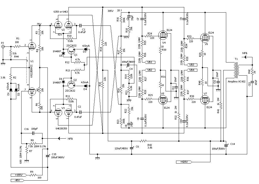
Fig.6 Amplifier circuit
Almost all resistors are metal film, I think carbon type will not suitable because the operating centre point may be changed too much.
The max voltage rating of the capacitor used for the lag-lead compensator is important. I choose the 500V rating mica capacitor, but 1000V may be better in ideal.
I cannot find such capacitor with good other characteristics and high reliability, unfortunately.
High rating capacitors are also required for the coupling capacitors of EL34 grid. Generally speaking, PP film capacitor has high voltage rating and good characteristics.
The coupling capacitor to the 2nd stage local feed-back allows lower max voltage, but the capacitance should be larger like this schematics, because of the feed-back stability.
There are three time constants in the feed-back loop, so please be care to the stagger ratio. So, the final coupling capacitor and resistor values are also important.
It may no need to explain about the 2nd stage cathode common should be constant current, because the load line will be "stand up" if resistor is used instead of constant current circuit, which brings higher distortion level.
However, if still you do not like to use semiconductors, that is your choice ;)
The feedback gain is almost -25dB in total, but -15dB is local feed-back. I want to get more deep feed-back, if I have 100mS ultra high gm triode :-)
And the closed loop gain is 17.5dB.
The ripple voltage of +B is added to the local feed-back as a common mode value, but two balanced differentials are opposite to the common mode, so ripple will not appear at the grid of final stage.
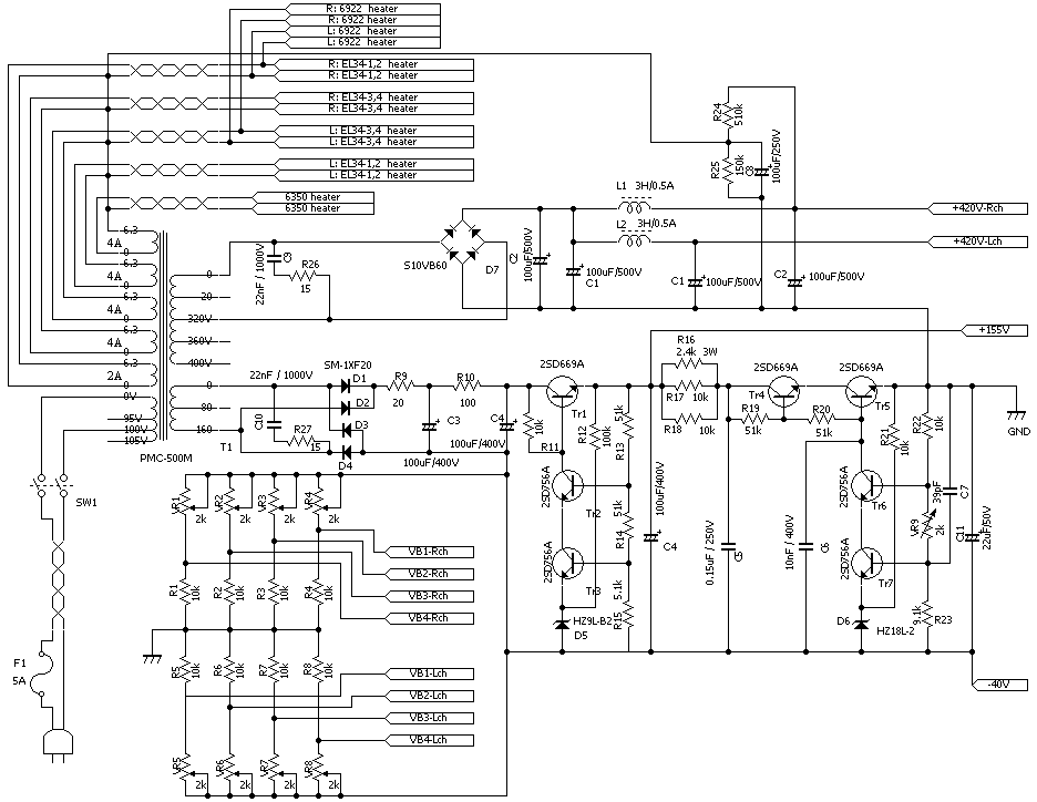
Fig.7 Power supply
I employed two inductors for stereo two channels, the reason is very simple, I cannot get enough current rating inductor in Japan. Of cause, cross-talk is one of the advantage by two inductors.
Please be care to the voltage to the capacitor, as it will be higher 20V or more before tubes are working.
If too high voltage, you can use higher voltage tap of primary winding, the magnetic flux density becomes lower and the temperature of iron becomes also lower, so it is safety.
Negative voltage power supply is shared by the 1st stage and final bias voltage. I use the rest voltage for the 1st stage anode power.
You may feel the negative voltage regulator is strange, but there is no problem. If you think that the voltage reference should be always ground, you cannot understand this method.
I have employed cascode structure for the voltage control transistor because of the max rating of transistor.
This is better for the reliability than high voltage transistor, as real SOA(Safety Operating Area) is wider.
I use small heat sink for these transistors.
Error amp is also cascoded.
And the big capacitor is used for the phase compensator. As the voltage of load resistor is very high, so the gain of error amp is also high, therefore the compensator time constant should be larger for stable feed-back.
The 1st stage noise is important for the 3 stages amp, as the open gain is so high.
I have employed the regulated power supply for the first stage, for this purpose.
I have employed the very high speed recovery diode for the 1st stage power, this is also important for low noise.
Please find here for the table of parts.
The output transformer that I employed is the Amplimo, which is designed by Mr. van der Veen and his transformer had took the world by storm once. The toroidal transformer characteristic is quite nice, and it is not expensive.
The max power rating of this transformer is 100W/30Hz, but it is defined at 8Ω and real impedance at low frequency is 6Ω, so allowable power will be more larger (or lower frequency if the same power).
And, feed-back stability is strongly related to the transformer as I already mentioned, which is calculated from the catalogue spec by the method of van der Veen's thesis.
Please find here in detail of the output transformer.
From the schematics, if you cannot understand how to adjust, I think you will not want to make such stupid amp, so maybe there is no need to write, but I write ;)
Of cause oscillo-scope is required for the adjustment. The feed-back can be easily unstable by the mounting or wiring, so you have to confirm the stability by yourself.
There are two types of parts, one is written is the schematics, and the other is the wire.
I bought the chassis at Noguchi-transformer shop, as they sell the custom chassis for their power transformer. It has a holes for the iron, so the handcraft is easy. A square hole is sometimes trouble and is labor. The material of this chassis is the 5052 Al-Mg alloy with 2mm thickness, but this is almost limit of handcraft. I had made punch holes by punching tool with big wrench, but its blade is finished to use ;)
The damping factor is almost 11. This value is higher than general tube amp, but I do not satisfied. I'd like to make 30 but open gain is not enough ;)
The distortion data is below. Certainly, this value is due to the feed-back method.
Non clip maximum power is 80W at 8Ω, so the THD became worse from 80W. Max power is around 100W if 6Ω load by the calculation, but I do not have a dummy load of 6Ω ;)
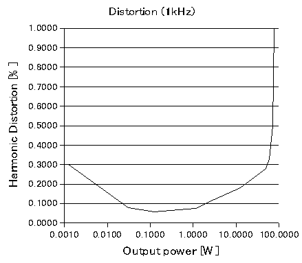
In practical, the maximum peak power when I listen is around 20W even when very loudly, so I think the distortion level is OK for me.
The noise level is less than 0.2mV at 10 to 200kHz range without any filters, so this is no problem.
The low frequency cross-talk is quite small (less than noise level), this depends on the individual power inductor per channel.
GREAT!
Here you can find some pictures.
I had found the issue of unstableness similar to the low frequency oscillation, and it seemed gradually to become unstable.
The sound was more distorted if I had connected with Volume control rather than the CD direct connection, so the grid current seemed to flow by the unstable contact of the tube socket at the first stage.
However, the oscillation is closely concerned to the sound level, and the symptom was quite rare at first but it becomes worse little by little. Firstly I have found this phenomenon, the oscillation was stopped after certain time, but the symptom became worse and worse.
Therefore, I considered there might be a complicated reason by several factors.
Then, I decide to fix and modify my amp as I have some ideas that I had better change in some points.
Modification points are below.
The reference of local feed back was changed GND to the Power supply of the first stage.
By this modification, common mode noise of the first stage will be suppressed.
The voltage regulator of the first stage had been required because of this local feedback,
so the regulator can be deleted by this modification in theory, but I leave as it is.
And, the capacitor which passed the signal to the GND is also deleted, so one questionable time constant(?) is also disappeared. (Although, this time constant is not significant for the feedback stability, because this capacitor is employed to suppress the common mode of feed back pass.)
The stability of the feedback path seems to be better by this modification, I can stop the very low frequency oscillating. Probably common mode noise from the feedback path may concerned to this phenomenon.
However, it could be unstable when high frequency square wave input (not always, but sometimes), especially at the corner edge of the square wave. So I changed some additional points to fix this issue.
The main reason of the high frequency oscillation written above had been this resistor value (R12 and R13 of Fig 6). Constant current was supplied to the second stage by the semiconductor circuit, and here I inserted the base resistor in order to suppress the parasitic oscillation, but it seems to work opposite way :(
The Transistor hFE will be lower at high frequency, and corner of the squire wave includes vary high frequency components, so the base current is increased at the edge of the wave, and then the base voltage was down, and then emitter voltage was lowered, then corrector current was changed.
It became stable if deleted this resistor, and could be more stable by adding the small capacitor for the base of transistor. (Although, normally this capacitor brings unstable ;)
As I mentioned before, I had changed the phase compensator when adjustment, and the capacitor values were different by Left and Right channel, but I restore this value as originally I designed.
In short, above modifications brings high stability and the phase compensator
should be the same.
In other word, I had used unnecessary tricks.
I have changed them from 510kΩ to 1MΩ, because slightly low frequency stability seems to be better.
However, depending on the dispersion of tube characteristics, unexpected results may be brought by this method, Because, it shows 0.7V or higher voltage for the both end of this resistor in some tubes, clearly this voltage is due to the grid current. (I do not mean that there is thermal runaway risk directly from this data. Bias voltage is -15V or more, so it will not occur, but far different grid voltage for differential amp is unpleasant)
I choose this method because of my parts in stock, but twice of capacitor may be better.
To tell the truth, when I made this amp, I had added the fan soon later around two month but I did not write it because it is troublesome to explain ;)
Additionally, this ventilating fan is not necessarily required. If you install the radiator at the outside of the chassis, it will be better for heat radiation.
I feel it is boorish and unromantic that we can find the radiator in outside, even I painted with "japan" with considerable effort, so I added the fan.
Incidentally, the temperature of the power transistor surface is around 90 °C when the ambience temperature of the transistor (which means in the chassis) is 25°C. The temperature in the chassis was around 45C or more without fan, but it becomes under the 40°C by the fan ventilation.
And, I had modified the ventilator to conduct the back lid. The employed fan is very quiet type, but the power supply voltage is reduced just the fan can be started to work.
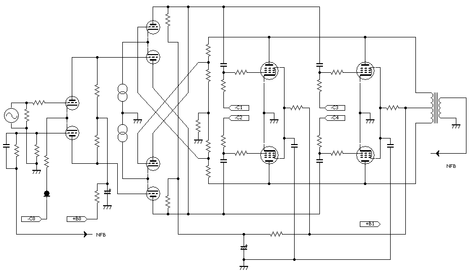
Here you can find the modified circuit.
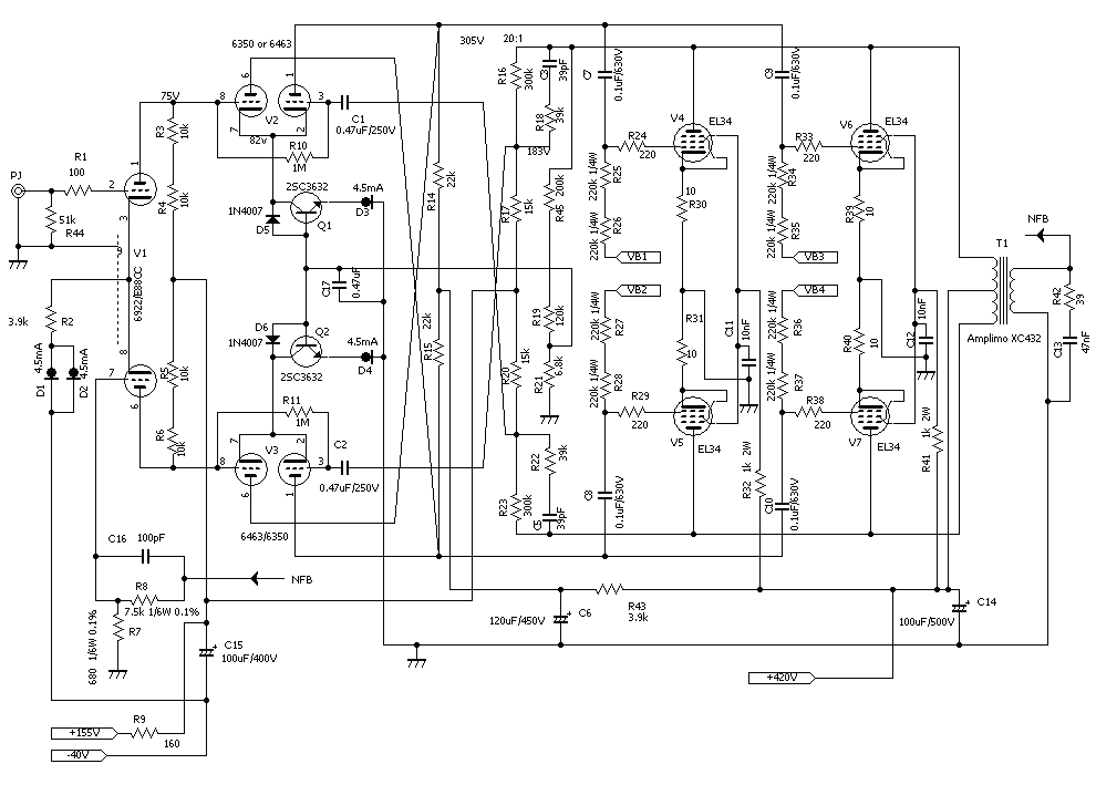 Fig.8 Modified circuit diagramme
Modified points are written above. C17 is the added capacitor written above.
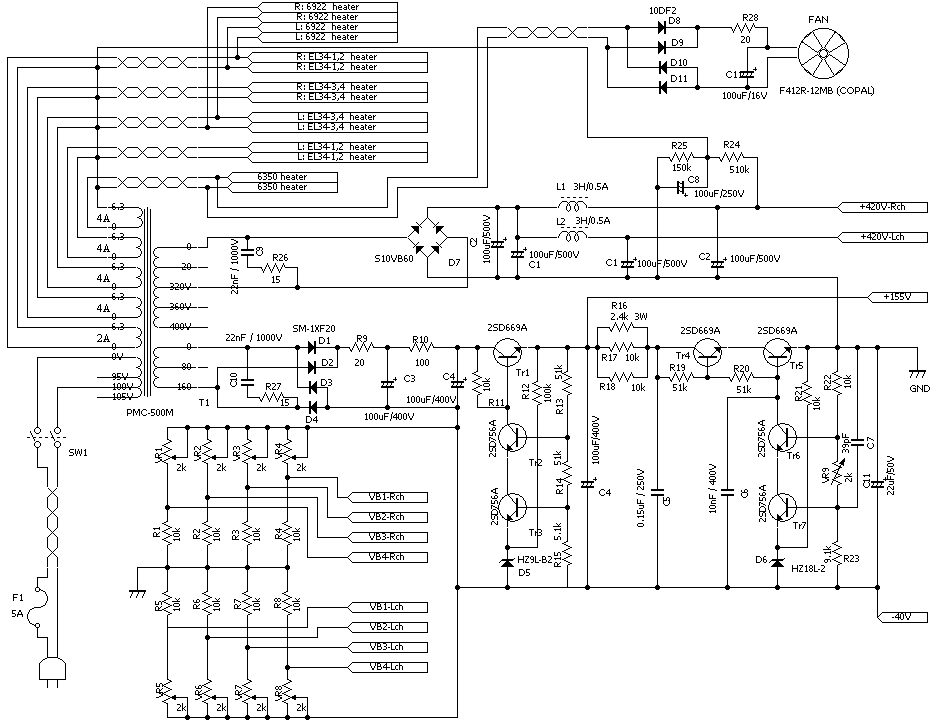 Fig.9 Power suppply with ventilation fan
You can use another type of ventilating fan if voltage is OK, but PC's one is not suitable because it is noisy.
Pictures are added to here.
Return to English Home